Tuesday, February 7, 2017

198322 : COMPUTER ARCHITECTURE

Member in Group 5

573040260-3 Kittipod Chantarasopon
573040314-6 Chanyanood Charoenkitsupat
573040647-9 Kamonlapop Kamta

573040673-8 นางสาวบุณยาพร พิมพะนิตย์
573040694-0 นางสาวศิริญา มหาโอฬารกุล
573040702-7 นายอภิสิทธิ์ คำยา

PENTIUM 4 AND POWERPC CACHE ORGANIZATIONDS

  • 80386 – no on chip cache 
  • 80486 – 8k using 16 byte lines and four way set 

associative organization

    Pentium (all versions) – two on chip L1 caches

  • Data & instructions 


    Pentium 4 – L1 caches

  • 8k bytes 
  • 64 byte lines 
  • four way set associative 

    L2 cache

  • Feeding both L1 caches 
  • 256k 
  • 128 byte lines 
  • 8 way set associative 


Figure 4.1 Pentium 4 Blocks Diagram

    Fetch/Decode Unit

  • Fetches instructions from L2 cache 
  • Decode into micro-ops 
  • Store micro-ops in L1 cache 

    Out of order execution logic

  • Schedules micro-ops 
  • Based on data dependence and resources 
  • May speculatively execute 

    Execution units

  • Execute micro-ops 
  • Data from L1 cache 
  • Results in registers 

    Memory subsystem

  • L2 cache and systems bus


Pentium 4 Design Reasoning

  • Decodes instructions into RISC like micro-ops before L1 cache
  • Micro-ops fixed length 
        Superscalar pipelining and scheduling

  • Pentium instructions long & complex 
  • Performance improved by separating decoding from scheduling & pipelining 
        (More later – ch14) 
  • Data cache is write back 
        Can be configured to write through 
  • L1 cache controlled by 2 bits in register 
        CD = cache disable 
        NW = not write through 
        2 instructions to invalidate (flush) cache and write back then Invalidate


PowerPC Cache Organization


    The PowerPC cache organization has evolved with the overall architecture of the PowerPC family, reflecting the relentless pursuit of performance that is the driving force for all microprocessor designers.

The original model

  • 601 – single 32kB 8 way set associative 
  • 603 – 16kB (2 x 8kB) two way set associative 
  • 604 – 32kB 
  • 610 – 64kB 
  • G3 & G4 
        64kB L1 cache – 8 way set associative

        256kB, 512kB or 1M L2 cache – two way set associative


PowerPC Internal Caches


Table 2 PowerPC Internal caches


PowerPC G4


Figure 4.2 Pentium 4 Block Diagram

    f
igure 4.2 Provides a simplified view of the PowerPC G4 organization, highlighting the placement of the two caches. The core execution unit are two integer arithmetic and logic units, which can execute in parallel, and a floating-point unit with its own multiply, add, and divide components. The data cache feeds both integer and floating-point operations via a load/store unit. The instruction cache, which is read only, feeds into and instruction unit, whose operation is discussed in Chapter 14.

    The L1 caches are eight-way set associative. The L2 cache is a two-way set associative cache with 256K, 512K, or 1MB if memory.


Comparison of Cache Sizes


Table 3 Cache Sizes of Some Processors


Reference: William Stallings. (2003). Computer Organization & Architecture DESIGN FOR PERFORMANCE(6th ed.):                    Pentium 4 and PowerPC Cache Organizations(pp 120-125). Upper Saddle River, NJ: Pearson

ELEMENTS OF CACHE DESIGN

    This section provides an overview of cache design parameters and reports some typical results. We occasionally refer to the use of caches in high-performance computing (HPC). Although there are a large number of cache implementation, there are a few basic design elements that serve to classify an differentiate cache architectures. Table 4.2 lists key elements.


Table 1 Elements of Cache Design


Cache Size


    The first element, cache size, has already been discussed. We would like the size of the cache to be small enough so that the overall average cost per bit it is close to that of main memory alone and large enough so that the overall average access time is close to that of the cache alone. Table 4.3 list the cache sizes of some current and past processors.


Mapping Function


    Because there are fewer cache lines than main memory block, an algorithm is needed for mapping main memory blocks into cache lines. Three techniques can be used: direct, associative, and set associative. For all three cases. The example includes the following elements:
  • The cache can hold 64 Kbytes.
  • Data is transferred between main memory and cache in blocks of 4 bytes each. This means that the cache is organized as 16K = 214 lines of 4 bytes each.
  • The main memory consists of 16 Mbytes, with each byte directly addressable by a 24-bit address (224 = 16M). Thus, for mapping purposes, can consider main memory to consist of 4Mblocks of 4 bytes each.
    
    Because there are fewer cache lines than main memory blocks, an algorithm is needed for mapping main memory blocks into cache lines. 

Three techniques can be used: direct, associative, and set associative

    Direct mapping, maps each block of main memory into only one possible cache line. Figure 4.7 illustrates the general mechanism. The mapping is expressed as


i = j modulo m

Where i = cache line number
      j = main memory block number
      m = number of lines in the cache


Figure 3.1 Direct-Mapping Cache organization[HWAN93]

    The effect of this mapping is that blocks of main memory are assigned to lines of the cache as follows


    Figure 3.2 shows our example system using direct mapping. In the example, m = 16K = 224 and I = j modulo 224. The mapping becomes as follows


Figure 3.2 Direct Mapping Example

    The direct mapping technique is simple and inexpensive to implement. Its main disadvantage is that there is a fixed cache location for any given block.

    Associative mapping overcomes the disadvantage of direct mapping by permitting each main memory block to be loaded into any line of the cache. Figure 3.3 shows our example using associative mapping.


Figure 3.3 Associative Mapping Example

    With associative mapping, there is flexibility as to which block to replace when a new block is read into the cache. Replacement algorithms, discussed later in this section, are designed to maximize the hit ratio.

    Set associative mapping is a compromise that exhibits the strengths of both the direct and associative approaches while reducing their disadvantages. The relationships are


m = v x k
i = j modulo v

Where i = cache set number
      j = main memory block number
      m = number of lines in the cache

    Figure 3.5 shows our example using set associative mapping with two lines in each set, referred to as two-way set associative


Replacement Algorithms


    When a new block is brought into the cache, one of the existing blocks must be replaced. A number of algorithms have been tried: We mention four of the most common. Probably the most effective is least recently used(LRU): Replace that block in the set that has been in the cache longest with no reference to it.


Figure 3.4 k-Way Set Associative Cache Organization


Figure 3.5 Two-Way Set Associative Mapping Example

    For 2-way set associative, this is easily implemented. Each line includes a USE bit. When a line is referenced, its USE bit is set to 1 and the USE bit of the other line in that set in set to 0. When a block is to be read into the set, the line whose USE bit is 0 is used. LRU should give the best hit ratio. First-in-first-out (FIFO): Replace that block in the set that has been in the cache longest. FIFO is easily implemented. Least frequently used(LFU): Replace that block in the set that has experienced the fewest references. A technique not based on usage is to pick a line at random from among the candidate lines.


Write Policy


    Before a block that is resident in the cache can be replaced, it necessary to consider whether in has been altered in the cache but not in main memory. If it has not, then the old block in the cache may be overwritten. A variety of write policies, with performance and economic trade-offs, is possible. There are 2 problems to contend with. First, more than one device may have access to main memory. A more complex problem occurs when multiple processors are attached to the same bus and each processor has its own local cache. Then, if a word is altered in one cache, it could conceivably invalidate a word in other cache.

    The simplest technique is called write through. Using this technique, all write operation are made to main memory as well as to the cache, ensuring that main memory is always valid. Any other processor-cache module can monitor traffic to main memory to maintain consistency within its own cache.

    In a bus organization in which more than one device has a cache and main memory is shared, a new problem is introduced. Even if a write-through policy is used, the other caches may contain invalid data. A system that prevents this problem is said to maintain cache coherency. Possible approaches to cache coherency include the following.
  • Bus watching with write through: Each cache controller monitors the address lines to detect write operation to memory by other bus masters.
  • Hardware transparency: Additional hardware is used to ensure that all updates to main memory via cache are reflected in all caches. 
  • Noncacheable memory: Only a portion of main memory is shared by more than one processor, and this is designated as noncacheable.

Line Size


  • Larger blocks reduce the number of blocks that fit into a cache. Because each block fetch overwrites older cache contents, a small number of blocks results in data being overwritten shortly after they are fetched.
  • As a block become larger, each additional world is farther from the requested word, and therefore less likely to be needed in the near future.

Number of Caches


    When cache were originally introduced, the typical system had a single cache.more recently, the use of multiple caches has become the norm. 2 aspects of this design issue concern the number of levels of caches and the use of unified versus split caches.
    
    Multilevel Caches
    
    As logic density has increased, it has become possible to have a cache on the same chip as the processor: the on-chip cache. Because of the short data paths internal to the processor, compared with bus lengths, on-chip cache accesses will complete appreciably faster than would even zero-wait state bus cycle.

    The inclusion of an on-chip cache leaves open the question of whether an off-chip, or external, cache is still desirable. The simplest such organization is known as a two-level cache, with the internal cache designated as level 1 (L1) and the external cache designated as level 2 (L2). Because if there is no L2 cache and the processor makes an access request for a memory location not in the L1 cache, then the processor must access DRAM or ROM memory across the bus. Due to the typically slow bus speed and slow memory access time, this results in poor performance. if an L2 SRAM (static RAM) cache is used, then frequently the missing information can be quickly retrieved. If the SRAM is fast enough to match the bus speed, then the data can be accessed using a zero-wait state transaction, the fastest type of bus transfer.

    Two features of contemporary cache design for multilevel caches are noteworthy. First, for an off-chip L2 cache, use a separate data path, so as to reduce the burden on the system bus. Second, with the continued shrinkage of processor components.

    The potential savings due to the use of an L2 cache depends on the hit rates in both the L1 and L2 caches. Several studies have shown that, in general, the use of a second-level cache does improve performance (e.g., see [AZIM92], [NOVI93], [HAND98]).


    Unified Versus Split Caches

    When the on-chip cache first made an appearance, many of the designs consisted of a single cache used to store references to both data and instructions. It has to split the cache into two: one dedicated to instructions and one dedicated to data.

    There are two potential advantages of a unified cache: 

  • For a given cache size, a unified cache has a higher hit rate than split caches because it balances the load between instruction and data fetches automatically. 
  • Only one cache needs to be designed and implemented. 
    Despite these advantages, the trend is toward split caches, particularly for superscalar machines such as the Pentium and PowerPC, which emphasize parallel instruction execution and the prefetching of predicted future instructions. The key advantage of the split cache design is that it eliminates contention for the cache between the instruction fetch/decode unit and the execution unit.This is important in any design that relies on the pipelining of instructions.

Reference: William Stallings. (2003). Computer Organization & Architecture DESIGN FOR PERFORMANCE(6th ed.):                    Elements of Cache Design(pp 108-119). Upper Saddle River, NJ: Pearson

CACHE MEMORY PRINCIPLES

    Cache memory is intended to give memory speed approaching that of the fastest memories available. The concept is illustrated in Figure 2.1


Figure 2.1 Cache and Main Memory

    When the processor attempts to read a word of memory, a check is made to determine if the word is in the cache. If so, the word is delivered to the processor. If not, a block of main memory, consisting of some fixed number of words, is read into the cache and then the word is delivered to the processor. There will be future references to that same memory locating or to other words in the block.


Figure 2.2 Cache/Main Memory Structure

    If a word in a block of memory is read, that block is transferred to one of the lines of the cache. Because there are more blocks than lines, an individual line cannot be uniquely and permanently dedicated to a particular block. Thus, each line includes a tag that identifies which particular block is currently being stored. The tag is usually a portion of the main memory address.

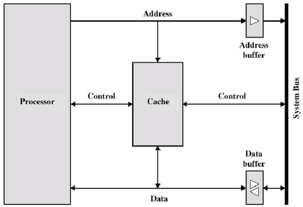
    Figure 2.3 illustrates the read operation. The processor generates the address, RA, of a word to be read. Figure 4.3 shown the last two operations occurring in parallel and reflects the organization shown in Figure 2.4, When a cache hit occurs, the data and address buffers are disabled and communication is only between processor and cache, with no system bus traffic. When a cache miss occur, the desired address is loaded onto the system bus and the data are returned through the data buffer to both the cache and the processor.


Figure 2.3 Cache Read Operation


Figure 2.4 Typical Cache Organization


Reference: William Stallings. (2003). Computer Organization & Architecture DESIGN FOR PERFORMANCE(6th ed.):                    Cache Memory Principles(pp 103-107). Upper Saddle River, NJ: Pearson

COMPUTER MEMORY SYSTEM OVERVIEW

Characteristics of Memory Systems


Key Characteristics of Computer Memory Systems


Location

  • Processor
  • Internal (main)
  • External (secondary)
    Internal memory is often equated with main memory. But there are other forms of internal memory. The processor requires its own local memory, in the form of registers. Cache is another form of internal memory. External memory consists of peripheral storage devices, such as disk and tape, that are accessible to the processor via I/O controllers.


Figure 1.1 Processor

Capacity

  • Word size
  • Number of words
    For internal memory, the capacity is typically expressed in terms of bytes (1 byte = 8 bits) or words. Common word lengths are 8, 16 and 32 bits. External memory capacity is typically expressed in terms of bytes.


Unit of Transfer

  • Word
  • Block
    For internal memory, the unit of transfer is equal to the number of data lines into and out of the memory module. This may be equal to the word length, but is often larger, such as 64, 128 or 256 bits.

    Word: The “natural” unit of organization of memory. The size of word is typically equal to the number of bits used to represent a number and to the instruction length. Unfortunately, there are many exceptions.

    Addressable units: In some systems, the addressable unit is the word. However, many systems allow addressing at the byte level. In any case, the relationship between the length in bits A of an address and the number N of addressable units is 2A = N

    For main memory, the unit of transfer is the number of bits read out of or written into memory at time. It need not equal a word or an addressable unit. For external memory, data are often transferred in much larger units than a word and these are referred to as blocks.


Access Method

  • Sequential
  • Direct
  • Random
  • Associative
    Sequential access: Memory is organized into units of data, called records. Access must be made in a specific linear sequence. Stored addressing information is used to separate records and assist in the retrieval process. A shared read/write mechanism is used and this must be moved from its current location to the desired location, passing and rejecting each intermediate record. Thus, the time to access an arbitrary record is highly variable. Tape units are sequential access.

    Direct access: As with sequential access, direct access involves a shared read-write mechanism. However, individual blocks or records have a unique address based on physical location. Access is accomplished by direct access to reach a general vicinity plus sequential searching, counting or waiting to reach the final location. Access time is variable. Disk units are direct access.


Figure 1.2 Disk

    Random access: Each addressable location in memory has a unique. Physically wired-in addressing mechanism. The time to access a given location is independent of the sequence of prior accesses and is constant. Thus, any location can be selected at random and directly addressed and accessed. Main memory and some cache systems are random access.

    Associative: This is a random-access type of memory that enables one to make a comparison of desired bit locations within a word for a specified match and to do this for all words simultaneously. Thus, a word is retrieved based on a portion of its contents rather than its address. As with ordinary random-access memory, each location has its own addressing mechanism and retrieval time is constant independent of location or prior access patterns. Cache memories may employ associative access.


Performance

  • Access time
  • Cycle time
  • Transfer rate
    Access time (latency): For random-access memory, this is the time it takes to perform a read or write operation, that is, the time from the instant that an address is presented to the memory to the instant that data have been stored or made available for use. For non-random-access memory, access time is the time it takes to position the read-write mechanism at the desired location.

    Memory cycle time: This concept is primarily applied to random-access memory and consists of the access time plus any additional time required before a second access can commence. This additional time may be required for transients to die out on signal lines or to regenerate data if they are read destructively. Note that memory cycle time is concerned with the system bus, not the processor.

    Transfer rate: This is the rate at which data can be transferred into or out of a memory unit. For random-access memory, it is equal to 1/(cycle time). For non-random-access memory, the following relationship holds: TN = TA + N/R
where 
TN = Average time to read or write N bits
      TA = Average access time
      N = Number of bits
      R = Transfer rate, in bits per second (bps)


Physical Type

  • Semiconductor
  • Magnetic
  • Optical
  • Magneto-optical
    The most common physical types of memory today are semiconductor memory, magnetic surface memory, used for disk and tape and optical and magnetic-optical.


Physical Characteristics

  • Volatile/nonvolatile
  • Erasable/nonerasable
    In a volatile memory, information decays naturally or is lost when electrical power is switched off. In a nonvolatile memory, information once recorded remains without deterioration until deliberately changed; no electrical power is needed to retain information. Magnetic-surface memories are nonvolatile. Semiconductor memory may be either volatile or nonvolatile. Nonerasable memory cannot be altered, except by destroying the storage unit. Semiconductor memory of this type is known as read only memory (ROM). Of necessity, a practical nonerasable memory must also be nonvolatile.


Figure 1.3 Read Only Memory (ROM)


Organization

    For random-access memory, the organization is a key design issue. By organization is meant the physical arrangement of bits to form words.


The Memory Hierarchy


Figure 1.4 The Memory Hierarchy

    As one goes down in the hierarchy, the following occur:
        a) Decreasing cost per bit
        b) Increasing capacity
        c) Increasing access time
        d) Decreasing frequency of access of the memory by the                  processor

    The fastest, smallest and most expensive type of memory consists of the registers internal to the processor. Typically, a processor will contain a few dozen such registers, although some machines contain hundreds of registers. Main memory is the principal internal memory system of the computer. Each location in main memory has a unique address. Main memory is usually extended with a higher-speed, smaller cache.


Reference: William Stallings. (2003). Computer Organization & Architecture DESIGN FOR PERFORMANCE(6th ed.):                    Computer Memory System Overview(pp 96-101). Upper Saddle River, NJ: Pearson